Introduction
Quality teams sometimes expect to see a “layer” left behind after laser cleaning—something they informally call a thermal expansion layer. Yet cross‑sections, EBSD maps, and hardness profiles often show no persistent band or altered microstructure in the base metal. Here’s the deal: when pulse energy, spot size, and scan strategy are chosen correctly, the energy is largely confined to contaminants and near‑surface films, not the substrate. That thermal confinement is why metallography frequently finds no heat‑affected zone (HAZ).
In this article, we connect the physics (absorption and thermal diffusion length), the parameter windows that prevent microstructural change, and the QA evidence that ties process inputs to metallographic outcomes. We’ll also clarify terminology: “thermal expansion layer” isn’t a standard metallurgical term. Instead, inspectors should use HAZ criteria—observable and persistent microstructural or property changes in the substrate.
Key takeaways
- Properly tuned laser cleaning confines heat to coatings/oxides; the substrate typically shows no HAZ in metallography.
- Thermal diffusion length scales with pulse duration; nanosecond pulses affect sub‑micron to a few microns, picosecond/femtosecond pulses confine to tens of nanometers.
- Safe windows depend on fluence, overlap, pulse regime, and scan speed/repetition rate coupling; these control thermal accumulation.
- QA alignment: expect no transformed band in cross‑section, EBSD metrics comparable to baseline, and microhardness within normal scatter.
Terms and context
Thermal expansion vs. metallurgical layers
Transient thermal strain or color changes from surface oxides can appear during cleaning, but they are not evidence of a metallurgical layer in the substrate. Metallographic evidence of a new layer requires a persistent change—e.g., a recrystallized or transformed band, resolidified film, or measurable property shift at the base metal. If none is present after proper etching, imaging, and hardness/EBSD checks, then there is no HAZ.
What constitutes a HAZ in metallurgy
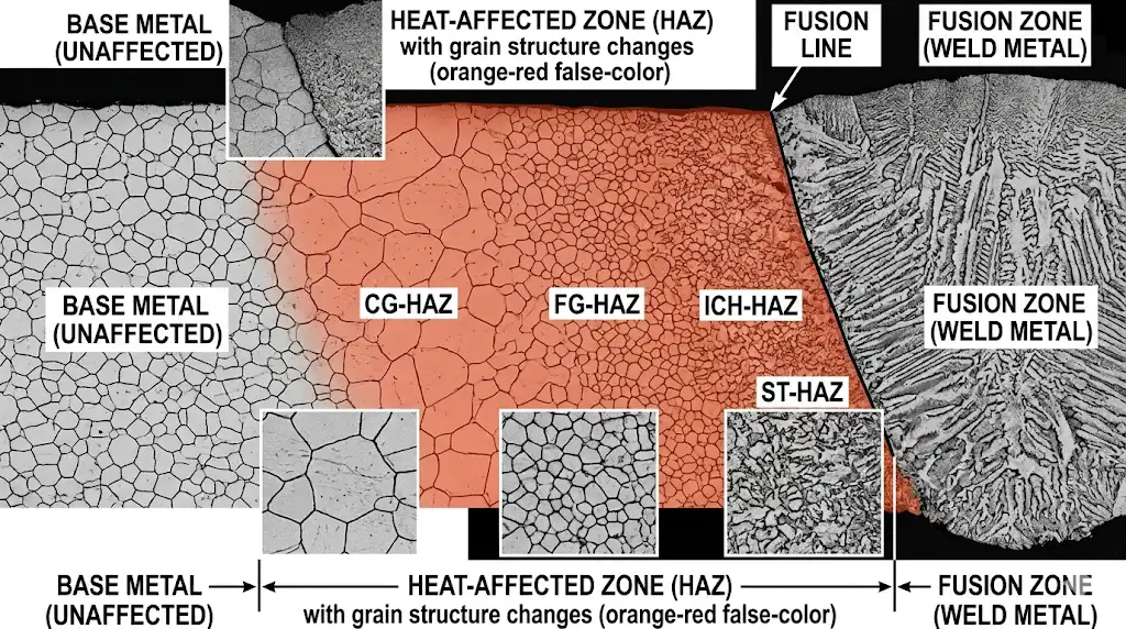
In welding and related thermal processes, the HAZ is the region of the base metal whose microstructure or properties have been altered by heat without melting. Acceptance logic commonly relies on cross‑sectional metallography, hardness traverses, and sometimes EBSD. For terminology context, see the ISO welding vocabulary (2019) entries in the online viewer, which codify HAZ concepts and related measures such as dHAZ diameter in resistance welding, as referenced in the ISO online browsing platform for welding terminology (2019). Practical acceptance frameworks that hinge on hardness limits are discussed by TWI (The Welding Institute); though aimed at welds, they illustrate how industry treats HAZ evaluation using hardness traverses—see TWI’s HAZ hardness compliance guidance (2008–2020 overview pages).
Laser–matter mechanisms
Absorption and selectivity at ~1 μm
At ~1064 nm (fiber/Nd:YAG fundamental), bare copper and aluminum are highly reflective, while steels absorb more strongly. Surface oxides, roughness, and temperature modify absorptivity, often aiding contaminant removal. For optical constants context, Johnson & Christy’s copper data as compiled by refractiveindex.info remain a standard reference—see Johnson–Christy copper optical constants (1972) on refractiveindex.info. The practical takeaway: different alloys and surface states load energy very differently; cleaning strategies must reflect that.
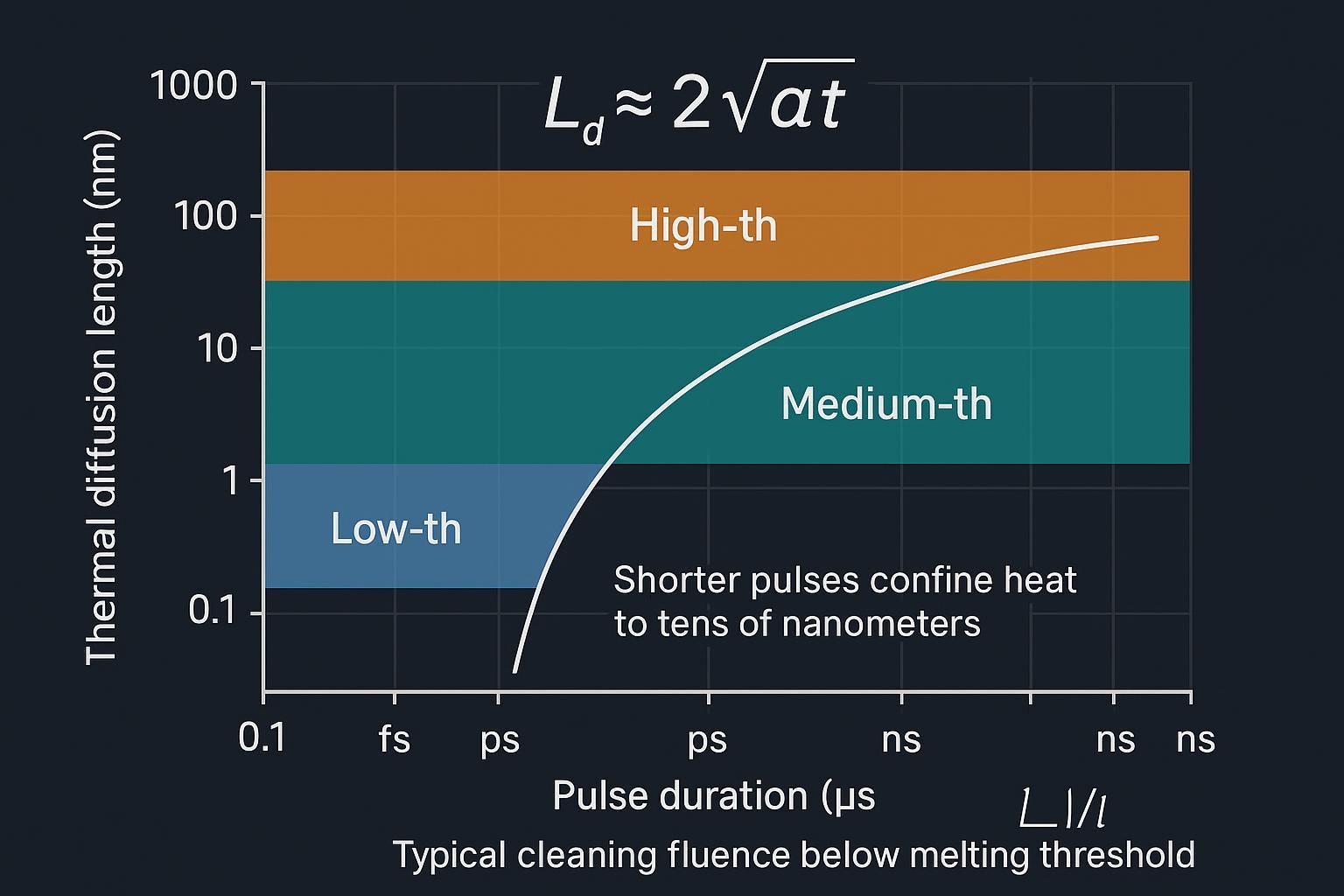
Thermal diffusion length and pulse duration
The characteristic depth scale for heat to spread during a pulse is the thermal diffusion length, which scales with pulse duration t and thermal diffusivity α. A common engineering form is:
L_d ≈ 2·√(α·t)For low‑diffusivity stainless (α ≈ 4×10⁻⁶ m²/s), L_d is roughly 0.4 μm at 10 ns and ~12.6 nm at 10 ps. For higher‑diffusivity aluminum‑like values (α ≈ 9.7×10⁻⁵ m²/s), L_d is ~2 μm at 10 ns and ~62 nm at 10 ps. These scales make it clear why picosecond/femtosecond regimes so effectively confine heat to the very surface, while nanosecond cleaning still stays within sub‑micron to a few microns when fluence is kept below melting thresholds. Engineering references for α and thermal conduction relations include the Engineering Toolbox conductivity/diffusivity overviews (general reference context, 2024).
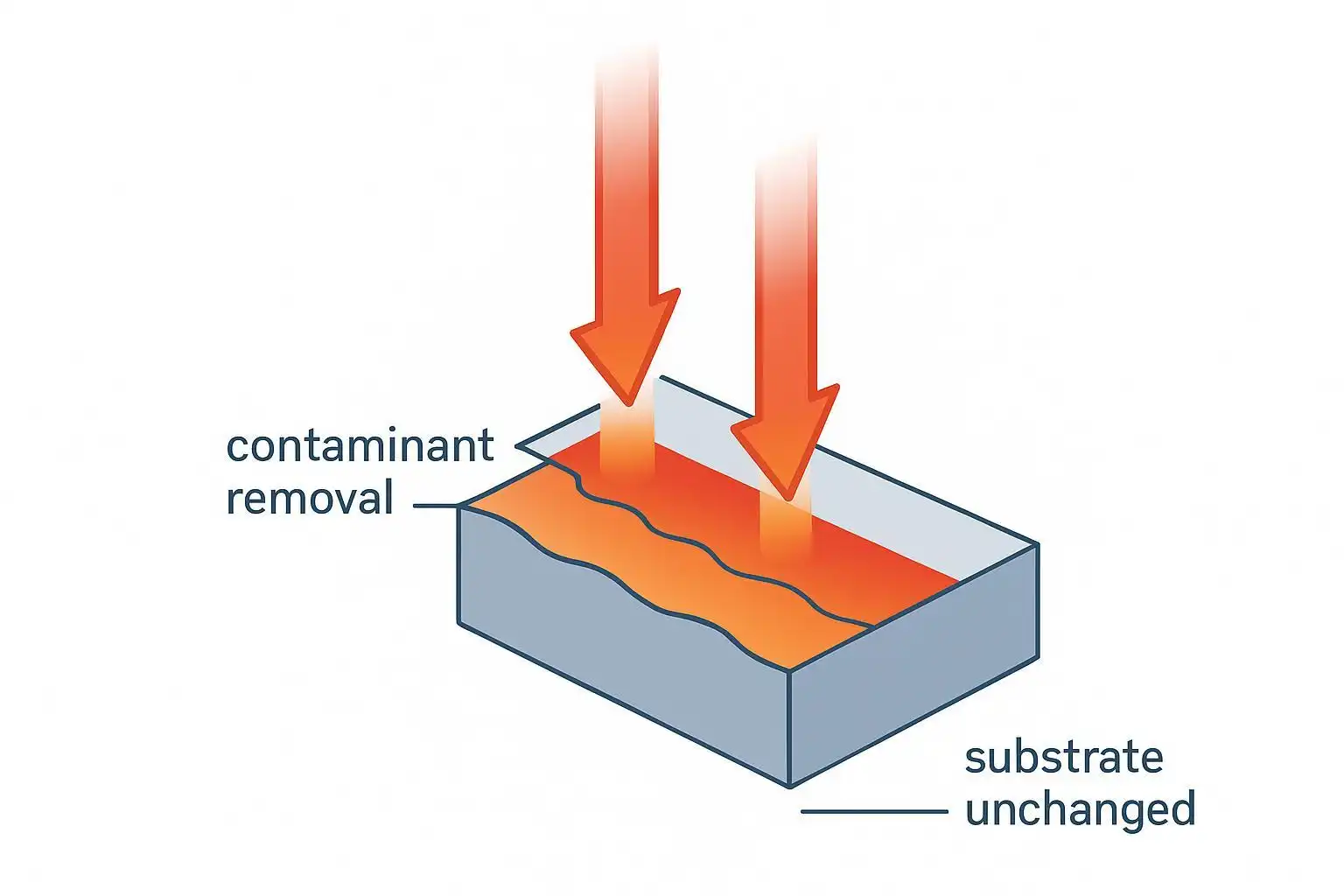
Photothermal, photomechanical, ablation roles
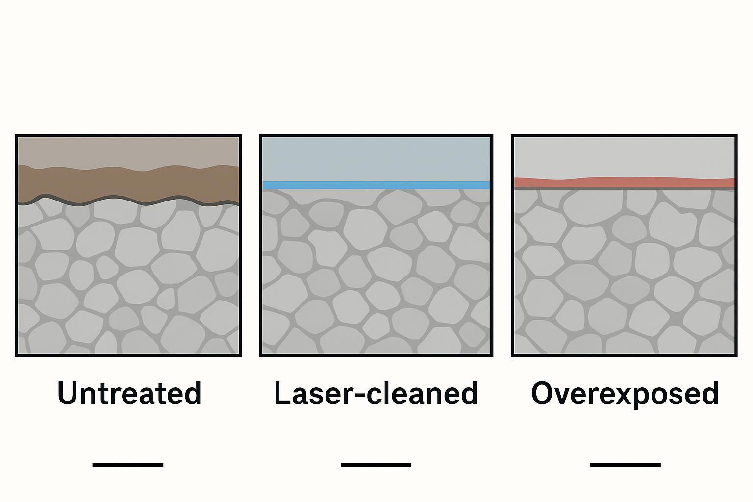
Contaminants and oxides can be removed by a mix of photothermal desorption, brittle‑film fracture from thermoelastic stress (photomechanical effects), and, at higher fluence, ablative ejection. The substrate remains unaffected when the interface temperature and stress do not exceed thresholds for melting, phase transformation, or plastic strain at the diffusion depth set by the pulse. Think of the process like popping a brittle glaze off a mug without heating the clay body underneath—brief, localized energy in the film, not the base.
Parameters that avoid substrate change
Fluence windows and overlap control
Cleaning operates in a fluence window high enough to break adhesion and eject films, yet below the onset of substrate melting. For steels, practical ns windows often sit in the O(0.5–2.5 J/cm²) range depending on spot size, coating type/thickness, and wavelength; reflective alloys may require smaller incremental steps with more passes. Overlap (pulses‑per‑spot) raises effective dose and temperature—so cap linear and cross‑hatch overlap to prevent accumulation, especially at edges and corners.
Pulse regime choice: ns vs. ps/fs
Nanosecond sources remain common for industrial cleaning due to cost and throughput. Picosecond/femtosecond systems further shrink diffusion length, reducing thermal load and the risk of rims on sensitive substrates or thin sections. If inspectors demand the lowest possible near‑surface thermal signature, ps/fs can be preferred—at the cost of system complexity and, often, throughput.
Scan speed and repetition rate management
Higher repetition rates with slow scan speeds can stealthily raise local temperature via pulse stacking. Couple scan speed to repetition rate to hold pulses‑per‑spot within your validated window, and add inter‑pass delays or alternate hatch directions to dissipate residual heat. Monitor geometry hot spots (fillets, steps) where beam footing changes.
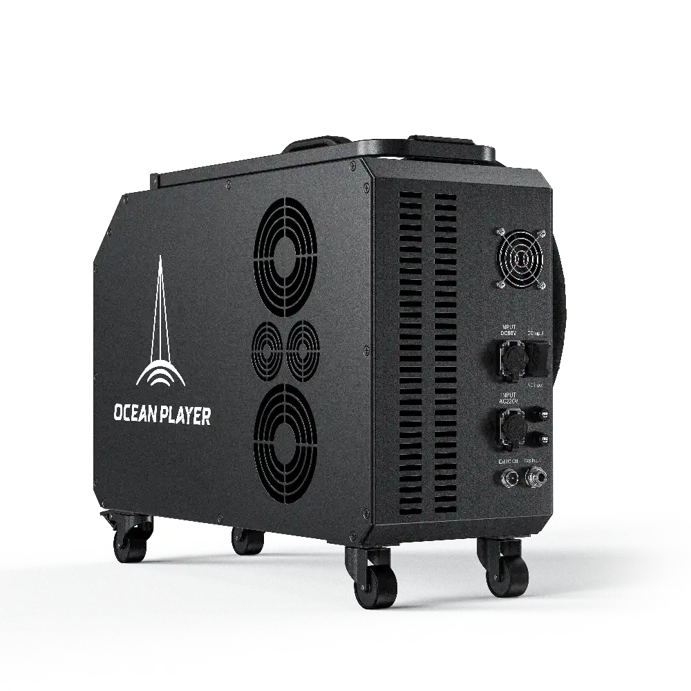
A brief, educational example of preset philosophy: Many industrial systems pair fluence caps with overlap limits and PRR–speed coupling to minimize substrate change. For example, preset recipes may constrain pulses‑per‑spot below an empirically validated threshold and lock hatch spacing to spot diameter so dose doesn’t creep. On modern units like Oceanplayer, application presets typically bundle these guards—fluence windows, overlap ranges, and scan‑speed/PRR coupling—so operators can remove rusts/paints while avoiding conditions that could form a thin remelt rim. These presets should still be validated by your lab with cross‑sections and hardness/roughness checks for each substrate/coating.
Metallography expectations
What optical/SEM/EBSD should (not) show
On properly cleaned samples, optical/SEM cross‑sections should not reveal a continuous remelt band, new transformed phase, or recrystallized layer at the base metal interface. EBSD maps near the surface should mirror polished controls: similar grain orientations, no abnormal grain refinement band, and KAM/GOS metrics within baseline scatter. When in doubt, tighten step size at the top few microns and document indexing rates.
Microhardness and roughness checks
Microhardness traverses (e.g., HV0.025–HV0.05) across the top 20–50 μm should be statistically indistinguishable from controls; practical acceptance is often phrased as “within typical baseline scatter” for the alloy and heat treatment. For surfaces heading to repainting or bonding, post‑clean Ra should sit within about ±20% of the pre‑clean baseline unless a mild texture is intentionally targeted to aid adhesion. Hardness‑anchored acceptance logic echoes industry HAZ practice as discussed in TWI’s overview of HAZ hardness acceptance (TWI, 2008–2020 pages).
Interpreting borderline surface features
If a thin, bright band appears at the very surface under high magnification or after aggressive etching, confirm with SEM whether it’s a genuine remelt rim versus an etching artifact or redeposited debris. Look for smooth re‑solidified morphology and a continuous band; if present, reduce fluence, lower overlap, increase scan speed, or shift to shorter pulses, then re‑validate.
Suggested QA recording format (keep concise and reproducible):
| Checkpoint | Method | Acceptance cue |
|---|---|---|
| Cross‑section | Optical/SEM | No continuous remelt/transformed band at substrate |
| EBSD (near surface) | KAM/GOS vs. control | Metrics within baseline scatter; no new refined band |
| Microhardness | HV line scan (0–50 μm) | Mean within baseline; no systematic shift |
| Roughness | Ra/Rz before/after | Within ±20% unless texture is specified |
Edge cases and mitigation
When excessive ns fluence causes a thin rim
Symptoms: a smooth, continuous band a few microns thick and a subtle microrelief at the surface. Mitigation: step down fluence, lower overlap (or widen hatch), raise scan speed, add inter‑pass cooling, or transition to ps pulses for sensitive parts. Re‑etch and re‑image to confirm.
Highly reflective substrates (Al, Cu)
Bare Al/Cu reflect strongly at ~1 μm. Strategies: start with lower fluence and more passes, pre‑condition surfaces (light oxide helps absorption), consider shorter wavelengths (e.g., 532 nm) when available, or deploy ps sources for tighter confinement. Optical constants context is summarized in Johnson–Christy copper data (1972); actual absorptivity varies with oxide/roughness.
Complex geometries and thermal accumulation
Fillets, steps, and recesses change effective spot overlap and can trap heat or ejecta. Reduce pulses‑per‑spot locally (dynamic speed boost), re‑sequence hatches to alternate directions, and insert dwell breaks on tight radii. Always validate representative features in cross‑section, not just flats.
Conclusion
Metallography often shows no HAZ after laser cleaning because properly selected fluence, overlap, pulse regime, and scan strategy confine energy to contaminants and near‑surface films while keeping substrate temperatures below transformation or melting thresholds. The non‑standard “thermal expansion layer” notion doesn’t apply; inspectors should look for actual microstructural or property changes. For QA, rely on cross‑sections, EBSD near‑surface metrics, microhardness traverses, and roughness checks tied to your baseline. Keep nanosecond cleaning inside validated fluence/overlap windows, couple scan speed to PRR, and reserve ps/fs when substrates or tolerances demand the tightest thermal confinement. With that approach, “laser cleaning HAZ metallography” inspections should consistently confirm substrate integrity for downstream coating, welding prep, or bonding.
References for terminology and physics context include the ISO online welding terminology viewer (2019), TWI’s HAZ hardness acceptance discussion, Engineering Toolbox thermal data (2024), and refractiveindex.info’s Johnson–Christy copper page (1972) for optical constants context.